Showing posts with label Materials Science. Show all posts

Thursday, June 19, 2014

Cold worked glass


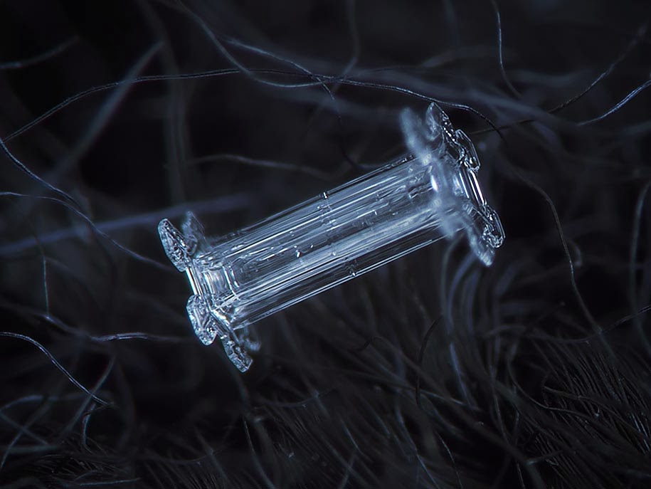
How a piece of cold worked glass looks like.

Friday, May 30, 2014

Quantum Dot Nanosensors for Visual Sensing

As we advance into artificial sensing technology, it is pertinent that use of such technology be made to advance the interests of humans in general and improve the quality of life. Such motives have mostly been the driving force of technologies. For what is invented for space exploration helps fight diseases on earth and other examples include what was designed for war later supplementing great engineering technologies. The end result is usually the driving force or as a side motive at minimum. The advancement of nanotechnology means much more components in the same space and hence much smaller equipments. Sensors, were they small enough, could be used to replace the complicated biological and natural sensors in humans or animals and even be given to computers and robots.

Usage of Quantum Dots explore such a use of a nanosensor and design it so as to restore the vision of visually impaired humans or give eyesight to computers; not using something as crude and huge in size as a camera or a lens rather targeting the core of sensing itself. Inherently, this research targets the retina itself. An artificial replacement for retina would enable humans to benefit from a restored vision without invasive brain surgeries. Computers, at the same time, will be able to detect photons with a much much greater sensitivity than a normal digital camera based optical detection method. Photo-detection needs a complicated device or materials engineered to the extent that the sensor would not be a physical obstruction in terms of its size when placed in the human eye or as an attachment to it as well as be biocompatible. To keep up with both these de facto requirements and many others implications of them, extensive study of the mechanism and biocompatibility has been done in research work for the selection of the materials and the literature shows an in-depth detail on why the materials chosen would make graphene and graphite based quantum dots a great candidate combination for such sensors. They can be used with two routes in the basic design; the generation of photocurrent via quantum dots on detection of photons or polarization of human nerves to fire neurons via quantum dots whenever photons are detected.


Works on the topic:

Cheng, Shih-Hao et al. All Carbon-Based Photodetectors: An eminent integration of graphite quantum dots and two dimensional graphene. Scientific Reports 3, Article number: 2694. Published: 18 September 2013.
Tang, L. et al. Deep ultraviolet photoluminescence of water-soluble self passivated graphene quantum dots. ACS Nano 6, 5102–5110 (2012).
Li, Y. et al. An Electrochemical Avenue to Green-Luminescent Graphene Quantum Dots as Potential Electron-Acceptors for Photovoltaics. Adv. Mater. 23, 776–780 (2011).
Li, X. et al. Large-area synthesis of high-quality and uniform graphene films on copper foils. Science 324, 1312–1314 (2009).
Katherine Lugo et al. . Remote switching of cellular activity and cell signaling using light in conjunction with quantum dots. Vol 3.(2012)
Quantum Dots – A Definition, How They Work, Manufacturing, Applications and Their Use In Fighting Cancer Printable Document. Online Document: Accessed on: 27 May 2014.
Lin, Rieke and Research groups. Quantum Dots and Cells. Website: Accessed on 27 May 2014.
K. S. Novoselov, A. K. Geim, S. V. Morozov, D. Jiang, Y. Zhang, S. V. Dubonos, I. V. Grigorieva, and A. A. Firsov, Electric field effect in atomically thin carbon films, Science 306, 666 (2004)
K. Novoselov, D. Jiang, F. Schedin, T. Booth, V. Khotkevich, S.Morozov, and A. Geim, Two-dimensional atomic crystals, Proc. Natl. Acad. Sci. USA 102,10451 (2005).
Carion O., Mahler B., Pons T., Dubertret B., “Synthesis, encapsulation, purification and coupling of single quantum dots in phospholipid micelles for their use in cellular and in vivo imaging,” Nat. Protoc. 2(10), 2383–2390 (2007).10.1038/nprot.2007.351
Chaoxu Li, J. A.. “Biodegradable nanocomposites of amyloid fibrils and graphene with shape-memory and enzyme-sensing properties”, Nature Nanotechnology, 421–427 (2012)
Kian, P. L., Qiaoliang, B., Goki, E. & Manish, C. Graphene oxide as a chemically tunable platform for opticalhttp://cdncache-a.akamaihd.net/items/it/img/arrow-10x10.png applications. Nat. Chem. 2, 1015–1024 (2010).
Galande, C. et al. Quasi-molecular fluorescence from graphene oxide. Sci. Rep. 1, 85 (2011).
Jingzhi, S. et al. The Originhttp://cdncache-a.akamaihd.net/items/it/img/arrow-10x10.png of Fluorescence from Graphene Oxide. Sci. Rep. 2, 972 (2012).
Sargent, E. H. Photodetectors: A sensitivehttp://cdncache-a.akamaihd.net/items/it/img/arrow-10x10.png pair. Nat. Nanotech. 7, 349–350 (2012).
Konstantatos, G. & Sargent, E. H. PbS colloidal quantum dot photoconductive photodetectors: Transporthttp://cdncache-a.akamaihd.net/items/it/img/arrow-10x10.png, traps, and gain. Appl. Phys. Lett. 91, 173505–173508 (2007).
Zhang, D., Gan, L., Cao, Y., Wanghttp://cdncache-a.akamaihd.net/items/it/img/arrow-10x10.png, Q. & Guo, X. Understanding Chargehttp://cdncache-a.akamaihd.net/items/it/img/arrow-10x10.png Transfer at PbS-Decorated Graphene Surfaces toward a Tunable Photosensor. Adv Mater. 24, 2715–2720 (2012).
Konstantatos, G. & Sargent, E. H. Nanostructured materials for photon detection. Nat. Nanotech. 5, 391–400 (2010).
Shen, J., Zhu, Y., Chenhttp://cdncache-a.akamaihd.net/items/it/img/arrow-10x10.png, C., Yanghttp://cdncache-a.akamaihd.net/items/it/img/arrow-10x10.png, X. & Li, C. Facile preparation and upconversion luminescence of graphene quantum dots. Chem. Commun. 47, 2580–2582 (2011)

Friday, April 25, 2014

Furnace simulation


As the research of Highbrows Engineering on furnace development specifically for Pakistani industry progresses, we would like to share it with every one else to keep it open sourced.

On the course of furnace simulation development, we have been reviewing and testing furnace simulators online and any options that might be there in the form of desktop applications so as to develop FurnoSim, the Pakistani bred industrial furnace simulator. The aim is to benefit both the industry as a commercial product as well as an academic product for students and professionals and it is on our to do list of products that are coming up.
Steeluniversity.org shares a free online furnace simulator which can calculate some basic cycles for some preset processes such as alloying. Although these do not cater the professional needs but they can be very exciting for fresh professionals or students to learn the processes without actually wasting energy and material. Go ahead and test their online electric arc furnace training simulator, for example. On the main page they also have other metallurgy and testing related simulation links that may come in handy for atleast learning and academic presentations.

On the side, keeping our promise of sharing the research with the world, our physics and electronics research side has been making progress and will be coming up with products soon. As a treat, a theoretical moving particle simulation is shared below with explanation:

This moving charge simulator shows for how +ive / -ive acceleration of electron emits light / radiation - fields point radially towards the charge and when the charge accelerates, the difference of where the charge should have been with previous velocity and where the charge is now with the change is a perpendicular shift of the field lines. This shift travels away form the charge at the speed of light as radiations. This can also be taken as a mathematical version of light where the light is considered as mathematical correction of the difference being updated through out the universe at the maximum speed possible (which is the speed of light). This changes with respect to relativity when you accelerate the electron to the speed of light and is also shown in the simulation (if you accelerate it to that point in the settings).

Monday, March 24, 2014

Nanotechnology for engineering applications


If you wish to deign alienware, you would be better off asking a science fiction author to suggest an approach for science. Which is why, yesterday's science fiction is today's technology.

A number of reasons have contributed to the fact that we are now looking towards the applications of smaller and smaller equipment. Nanotechnology can be used to compliment almost any other technology as it allows for 'more' literally. In some cases, nanotechnology is needed simply because only a component that small could fit in there without much disturbance or due to physical dimensions. Nanometer scale sensors make the possibilities of even the craziest ideas look real.

The idea of nano robots is one of the factors that drives nano scientists' motivation. It might be extremely useful to create a nano robot that is equipped with a nano scale sensor to measure localized real time stresses in structures. Structural integrity of a engineering equipment, constructions and large sized installations is vital in most cases. Materials engineers usually have to perform non destructive and destructive tests time and again to make sure that the structure will hold. This results in a lot of man hours and expenses. Furthermore, it is mostly mixed qualitative and quantitative decision by the engineer about when the structure needs to be reinforced, totally replaced or retested for cracks or failures again. An engineer might be wrong (human error) and might delay the test above a duration before which the structure might fail or the engineer might wrongly predict the duration period itself. This can result in catastrophic structural failures and result in either the equipment being shut down / totally replaced or even accidents.

To avoid such errors and to further add continuous monitoring, nano sensors can be placed within the structure itself which can then monitor the structure for local stresses. The combination of local stresses at different point can then give the overall view of stresses in the structure. When nano sensors are placed within the structure itself and are able to send the data to a monitoring computer, it would be able to not only monitor the real time stresses of the structure, but it would also give statistics for how the structure is used, what tasks put the most amount of stresses (and hence fatigue) on the structure. A higher fatigue would mean a higher degradation and early failure of the structure. Such statistics from actual real time monitoring rather than by timed testing can be of more use. As compared to the timed and scheduled testing, real time monitoring will give usage data of each second, enabling the computer to plot a graph of the statistics. This data will help engineers decide how to best use their equipment so that its structure gets minimum fatigue. In short, this will result in optimization and minimum wastage.

This can be easily done by using nano sensors that detect stresses. Piezoelectric materials would be a good category to start looking for the possible implementation materials and designs as they convert compression and tension into electricity (that can be used as the signal for computer to interpret).

Sunday, February 9, 2014

Smell of new electronic equipment


A question I was asked a few years ago; what is the familiar smell in all electronic stores and in new electronic equipment. I asked some electronic engineers, they didn't know anything specific and had different theories about it. Then I came across a few concepts of electronic materials which I compiled to suggest the most precise reasons possible.

Smell of new electronic equipment (almost similar or atleast recognizable) depends on these major factors:
  • Capacitor compounds.
  • Lead vapors in small amounts from soldered points.
  • Silicone (which is used in coating silicon wafers or protecting/damping circuits) "Cures" itself by reacting with moisture in the air to for acetic acid (smells a bit pungent like car hydraulics).
  • Ozone in small amounts (in case they are ON).
(In old and running equipment it might be burning dust.)

...a mixture of above smells in variable quantities attributes to the smell of new electronic equipment. Smell might vary to some extent as the quantity of each factor changes.
Different compounds used in the manufacturing contribute in both old and new equipment. Adding ozone if its on and dust in old or stored new one. It's ozone that makes the rodents afraid to dwell behind the 'ON' electronic equipment. Ozone is toxic for humans too so sleeping while there's something sparking in a circuit board is dangerous.

I think present analyzers have the capacity to check which type of vapours are present in any air sample and this could further be verified.

Thursday, January 23, 2014

Why do tubelights make noise?

If you ever wondered why does your tube light or other fluorescent lights make noise (often noticeable in a quiet room and sometimes even in normal background noise in case of old lights). The reason magnetostriction. When current moves through coils or wires, magnetic field is produced with it. This magnetic field causes the material to magnetic and demagnetize (and in case of alternating current (AC) at the frequency of ~50Hz). During the process of magnetization and its reversal, the magnetic domains change their orientation and hence the material changes dimensions to some extent.

This change due to rotation of magnetic domains to align with the magnetic field causes the material to vibrate at hence causing the noise. This is generally the noise that we hear from the tube lights, but one man's limitation is another man's sensor. This effect can be used to create magnetostrictive materials that act as sensors or actuators.

Note (from Wikipedia under creative commons share alike license): Most magnetic materials are polycrystalline, composed of microscopic crystalline grains. These grains are not the same as domains. Each grain is a little crystal, with the crystal lattices of separate grains oriented in random directions. In most materials, each grain is big enough to contain several domains. Each crystal has an "easy" axis of magnetization, and is divided into domains with the axis of magnetization parallel to this axis, in alternate directions.

Why do two parts of a broken magnet repel each other?

When you break a magnet, it often seems that the polarities have flipped.
This doesn't actually happen.
 
No polarity reversal occurs when you think the poles have flipped
- you are dealing with a magnet that has an axial field 
(pointing out through the flat face.) When you break 
it, each half has similar field, pointing in the same direction, which 
is unstable. One piece will want to flip so that the fields line up 
anti-parallel (lower energy situation).  
 
Whether the broken magnet attracts or repels each other depends
on how the poles were previously present.

If the original magnet looked like
  +-----------------------------+
N |                             | S
  +-----------------------------+ 
 
After it's broken, it becomes
  +-----------+     +---------------+
N |           |S   N|               | S
  +-----------+     +---------------+ 
 
The two broken parts will attract each other.

However, if the original magnet looked like:
(poles on the flat faces of the magnet)

                N
  +--------------------------------+
  |                                |
  +--------------------------------+
                S

After it is broken, it becomes


         N                    N
  +---------------+   +-----------------+
  |               |   |                 |
  +---------------+   +-----------------+
         S                    S

Therefore the two parts will repel each other and will try to invert.

These are only two simple cases. In reality, the poles
of a magnet can be more complicated. This just illustrates how the poles
affect behavior of magnets.

Wednesday, December 18, 2013

Tensile testing a single molecule

Nanotechnology has enabled things like Atomic Forced Microscopy (AFM) to benefit materials scientists and engineers but there's a use of the same equipment a materials engineer would find extremely amazing and would probably not have thought of using AFM for; tensile testing a single molecule.

This can be done by combining AFM with a piezoelectric positioner. under the cantilever probe of the microscope. The molecule once attached / bound (chemically or otherwise), at one side to the probe and the other side to the positioner, can be stressed by the piezoelectric material which will change height with application of electricity and the tensile testing data will be recorded by AFM's sensors. Now how much information can be acquired by tensile testing a single molecule alone puts materials engineering to a nano scale perspective against the bulk and the macro properties which are often completely different.


Basic operation of the AFM. As the AFM cantilever probes the surface by moving its tip along its contours, or when it pulls on a protein, the movement of the cantilever is detected with a laser beam that is focused to beam to the head of the cantilever and refracts into a photodetecter. The movement, or deflection, of the cantilever deflects the laser correspondingly, and this creates an image or produces other data about the surface or the sample (which may be a molecule). In single molecule force spectroscopy, the cantilever is pressed against a layer of proteins attached to a substrate, and the tip adsorbs a single protein molecule, which is then extended. Extension of the molecule by retraction of the piezoelectric positioner results in deflection of the cantilever. [Oberhauser et al. PNAS (January 2001), Vol. 98 (2): 468-472]


Sunday, December 1, 2013

Quantum confinement


Quantum confinement is to limit the size of the waves like you do in a guitar string by shortening the size of the string with your finger. Only in this case you are doing the same to the wave of light by limiting the wave by decreasing the size of the material to nano scale. That effect results in a change in the colour being emitted given that the colour differences are there due to the change in wavelengths. Hence you are getting a variety of different colours from the same material just like you can get a variety of tunes from the same string by shortening its length by holding it. This can have a wide range of applications (including sensors).

But why does nano gold look red when red has a longer wavelength than yellow? Shouldn't it shift to a colour with smaller wavelength due to quantum confinement? Here's a little Q/A session I had with Professor Daniel Mittleman of RICE University that clears things up a bit further with regard to gold being red in colour as nano particles and metals behaving in similar scenario:

Professor Mittleman: The reason that a chunk of gold is gold-colored has to do with the electronic level structure of the metal. In other words, it is a quantum effect, not easily explained by ordinary classical physics. 

When you make gold small, there are additional effects, completely unrelated to the electronic level structure, which dictate the color.  In other words, the reason that macroscopic gold is gold-colored has essentially nothing to do with the reason that nano-gold is red.  It is not as if this is a shift from yellow to red - instead, it is a completely different mechanism.  In the case of a metal like gold, the mechanism is the excitation of a plasmon, which is a collective oscillation of all the electrons in the nanoparticle.

The brief description of quantum confinement is applicable to semiconductors, where the number of free electrons is small (e.g., one per nanoparticle). When you have just one electron per nanoparticle, the dominant issue is the energy for that electron to be excited or de-excited - that is, the quantum confinement effect.  On the other hand, in a metal the number of electrons is large, even in a nanoparticle (e.g., one per atom), so the description is understandably quite different.  In that case, the electrons do not need to be excited out of chemical bonds in order to be free, so the energy of excitation is no longer an issue.  Instead, you have the possibility of having all the electrons oscillating together, like water sloshing back and forth in a jar.  That's a plasmon.  And that's why nano-gold is red.

Me: So does this mean that metals in general are exceptions to quantum confinement at nano scale given that metals will generally have much more than 1 free electron per nano particle or does this stand for gold only (why not other metals if in this case)? In short, the plasmon concept supersedes in case of all metals?

Secondly, does quantum confinement still have a partial effect on the net result when talking of gold? As in, a participation to a minor extent as the size of the particles still has been reduced? Or does quantum confinement has no effect at all in case of gold for the reasons you gave (having more free electrons) and the change in colour is fully credited to plasmon?

Professor Mittleman: To answer your specific questions:

1. I would not say that metals are an exception.  I would say it a slightly different way.  In semiconductors, the natural size of an electronic excitation (which is really both an electron and a hole, not just an electron) is in the range of 10 nanometers or larger, so quantum confinement is a big deal when your particle size is in that range.  In contrast, in metals, the effective size of a free electron is much smaller, so that they still behave the same even if the metal particle is only 2 nanometers across - they don't feel 'squeezed' at all by the small size of the particle, since they're smaller. Pretty much any metal will exhibit plasmon effects, similar to gold.  Gold is the one we talk about most often because it is one of the easiest nanoparticles to make.  But color changes due to plasmons can be seen in any nano-metal.
2. The change in color of metal nanoparticles is entirely due to plasmonic effects.  (Well, I guess I should say "almost entirely" just to hedge my bets, but I think it is really entirely.)  In other words, you can describe the change in color using purely classical physics, with no quantum mechanics at all (since plasmons are essentially a classical phenomenon).  Quantum confinement (in semiconductor particles) cannot be described using classical physics, so it is really a different thing entirely.
Now the question is how does quantum confinement affect the colour when the the applications of such do not actually go below the size of the atoms (which is ~ 0.1 nm) and actually don't directly squeeze the emission at atomic level? The relation is similar to a skier sking on a mountain and the height of the mountain. In this analogy, electron is the skier ofcourse. This can also be defined in semi conductors in relation to the exciton created by the absorption of light when electrons jump from their valance state to conducting state by absorbing energy. The electron leaves behind a hole and either drifts apart from it due to voltage or the hole and the electron start to orbit each other, hence creating an exciton. These excitons are much larger than a hydrogen atom and are the physical entity being directly affected by the quantum confinement in such cases as they may range from 2.3 nm (in ZnO) to 46 nm (in PbSe). Quantum confinement here directly affects their size and hence the levels at which they can exist due to the size of the material and this changes the colour the emit from red to green and to blue as the size gets smaller. This is also used to create 'quantum wells' by trapping excitons of different energy levels (say red trapped in green) in each other so that they can only travel in their plane and not in 3D. What use is a quantum well to us? They have a wide range of applications starting from DVD and CD lasers as well as the coloured (eg. red) lasers in laser pointers. Mass manufacturing the quantum well lasers are set of parallel processes which makes them inexpensive; a few rupees a piece.

Multiple uses and effects:

  • Quantum confinement in 3D; quantum dots, can be used to form optical fibres with near zero energy loss (hence data loss) over long distances making a possibility for extremely reliable and high data transfer rates.
  • Quantum confinement in 2D; quantum wires, to solve the 'wiring problem' in nanotechnology where we have the nano components but are limited to wire them using larger sized wiring, to create P-N junctions and hence transistors in a whole new paradigm or even to be used as sensors.
  • Quantum confinement in 1D; quantum wells, can be used to create lasers and other light emitters as explained above.

Quantum confinement as a nano-physics concept can be applied to engineering applications that make life easier and technology the high end either in designing sensors or otherwise. Pakistan should soon take up its role on the high end of technology as these are concepts not far from the grasps of Pakistani engineers.

Friday, November 22, 2013

Crystallography: Snowflakes

Images shared via Alexey Kljatov.

A Russian photographer, Alexey Kljatov created a self made camera-lens combination to take some inexpensive photographs of snowflakes that clearly show the crystallographic structure of each flake.

With each flake having undergone different thermodynamics, no two flakes are alike. What is interesting is that each flake shows the basic most thermodynamic concepts with respect to crystallography at a macro level.

The dendrites grow spaced from each other like leafs on a branch instead of a single solid being frozen because, at the seed's surface and the part yet liquid (solid-liquid interface) at the center, the temperature higher than it is in the solid or liquid due to temperature inversion. This means not only the dendrites tend to equally space away from each other but also grow further away from the interface deep into the liquid depending on the time they get to freeze. This results in the dendrites growing in a pattern of branch and leaf like structure so well, almost as if it was calculated before it was made. Well not almost... it was naturally calculated before it formed. It's thermodynamics in action. During freezing the latent heat of fusion given away by the freezing material is being exchanged at the solid-liquid interface which results in inversion of temperature in this region. The inversion simply denotes the raise in temperature above the freezing point as well as the ambient liquid temperature at the interface. Instead of the inversion of temperature slowing down the process, it instead gives the process a pattern. The material does not wait for this temperature to lower down as it finds a freezing opportunity on as a separate dendrite. Crystal starts forming and growing in shape of dendrites. Depending on what the localized thermodynamic conditions were, each flakes forms in different sizes and shapes, which is remarkably shown in the photography.


Tuesday, November 19, 2013

Energy Harvesting: Self Sufficient Technologies

When we talk of going green, using solar, wind and other 'green' technologies, mostly we are unknowingly talking about energy harvesting. Harvesting energy from ambiance might be a solution that has been staring at us since a long time. We can totally eliminate the need for powering our electronics with external sources; batteries or fuel. There are a multitude of methods well within our capabilities.

Pakistan can take a great boost by starting with the small but numerous devices. The multitude of dry batteries that we import would not even be needed. A TV remote control can be powered by the same energy that we apply to press the 'button' if we use a piezoelectric material which converts the movement into enough voltage to send the signal. Powering handy devices with body heat, solar cells, piezoelectrics, or even use the excessive background noise that we have in form of radio waves and wifi signals on hundreds of channels to power devices.

On a macro-scale, The vast deserts are a good source of solar, wind and other forms of energy harvesting. Also, humans had always been having good living conditions prior to advent of electricity. Passive solar building design can take down the carbon foot print of a building to near zero.

It's time Pakistan takes steps towards such technologies. It might seem that highly developed nations develop such technologies and then it is transferred to us, but the truth is, most innovative and energy efficient technologies come from developing countries because they have to make do with the least possible resources. There is a huge range of technologies which were either developed for or by developing nations and later introduced to the developed ones.


As I explained in the last post about programmable materials, the processing of information is being decentralized to make it more viable... the power overload may not be any different from the information overload. The fact is, we do not need to reduce our energy consumption, we just need to reduce the wastage. Recycling and harvesting the wasted energy and making most devices self sufficient in regards to power is the obvious solution.

Sunday, October 6, 2013

Material Intelligence: The Programmable Matter

The new era is an epoch of smart materials where materials and non living things can have intelligence without any circuits, processing power, mechanical gadgets involved - it comes directly from the materials properties at nano-scale. Intelligent materials are being developed for a lot of purposes and include functionalities like:
  • Piezoelectric materials - convert vibrations to electricity and converse.
  • Shape memory alloys - remember their shape at temperature zones.
  • Magnetostrictive materials - reshape under magnetic influence and converse.
  • Magnetic shape memory alloys - change shape under significant magnetic field.
  • Magnetocaloric materials - reversibly change their temperature in ratio to magnetic field.
  • pH-sensitive polymers - change their volume with ambient pH.
  • Temperature responsive polymers - respond to temperature changes.
  • Halochromic materials - change colour with acidity.
  • Chromogenic systems - change colour with electricity, heat or light. LCDs use such materials.
  • Ferrofluids - strongly magnetizable fluids just by presence of magnetic field.
  • Photomechanical materials - change shape with light.
  • Polymorph materials - mold with hot water.
  • Self-healing materials - heal their own wear and tear.
  • Dielectric elastomers -  produce high strain with electricity.
  • Thermoelectric materials - convert temperature difference to electricity and converse.

This opens the doors to a new science of programming matter itself. Using any combination of materials above or other such materials it is possible to program the material to achieve basic functionalities that would normally take a computer processor or human brain to perform. A BBC news article mentions discovery of shape memory alloys that can be reshaped indefinitely by heating and cooling without wear and tear. The martensite structure of the shape memory alloys allows the materials to 'decide' conditionally and by the use of conditional programming of the materials they can be used to perform functions like automatic window openers or even as the means to guide solar panels on the Hubble Space Telescope to always point towards sun.

The programming of materials opens a front at nano-scale physics that uses the skills of computing and materials science to acquire results with no complexity at the macro level.

Saturday, August 17, 2013

Earth sniped


A satirical depiction of how it would look to an astronaut on the Moon if earth gets hit by an ultra hard asteroid at an ultra high speed. A better satirical caption would be, "...all my stuff was there!"

Wednesday, August 14, 2013

Electromagnetic Pulse Capacitor Comparison

Happy independence day to all Pakistanis. As a independence day gift, we are releasing high tech interest base research on electromagnetic pulse as a part of this blog.
 

Electromagnetic Pulse


The term electromagnetic pulse (sometimes abbreviated EMP) is a burst of electromagnetic radiation that results from an explosion (usually from the detonation of a nuclear weapon) and/or a suddenly fluctuating magnetic field. The resulting rapidly changing electric fields or magnetic fields may couple with electrical/electronic systems to produce damaging current and voltage surges.

In military terminology, a nuclear bomb detonated hundreds of kilometers above the Earth’s surface is known as a high-altitude electromagnetic pulse (HEMP) device. Nuclear electromagnetic pulse has three distinct time components that result from different physical phenomena. Effects of a HEMP device depend on a very large number of factors, including the altitude of the detonation, energy yield, gamma ray output, interactions with the Earth’s magnetic field, and electromagnetic shielding of targets.

The case of a nuclear electromagnetic pulse differs from other kinds of electromagnetic pulse (EMP) in being a complex electromagnetic multi-pulse. The complex multi-pulse is usually described in terms of three components, and these three components have been defined as such by the international standards commission called the International Electrotechnical Commission (IEC).

The three components of nuclear EMP, as defined by the IEC, are called E1, E2 and E3.

Capacitor Comparison for EMP use:
    • Ceramic capacitors range from low to high voltage but are vulnerable to aging (and change in crystal structure over time) and have to be reheated up to curie point to reverse the aging effect.
    • Polymeric capacitors produce up to 60,000V but temperature stability is poor; inappropriate for radio frequency applications due to excessive dielectric heating.
    • Glass Capacitors although have a high working temperature and are very stable but their capacitance is in picofarads.
    • Ultra-capacitors have a maximum working voltage upto 24.4 V and hence need a large amount to series connections to build up an EMP device.

      Class II ceramic capacitors provide bet material for the EMP effect to successfully occur over a voltage of ~ 50,000V.

      To further improve the dissipation rate electrical grade castor oil or similar high dielectric constant fluid can be used along with extended foil plates in combination with the ceramic capacitors to use their high voltage to generate EMP.

      Thursday, July 25, 2013

      Researchers create ‘an impossible material’ by mistake

      shared via io9 and plosone under creative commons license.

      In yet another example of scientific serendipity, Uppsala University researchers have created an unprecedented material with record-breaking properties. And most remarkable of all, this new material — which was thought impossible to make for over a century — was the result of an accident in the lab.

      And indeed, the new magnesium carbonate material exhibits some remarkable properties.

      Adsorption, Not Absorption

      Called upsalite in honor of the university where it was discovered, the material features a surface area of 800 square meters per gram. It's got the highest surface area measured for a synthesized alkali metal carbonate. And in addition, upsalite is filled with empty pores all having a diameter smaller than 10 nanometers.

      This means that it can absorb — or more accurately, adsorb — more water at low relative humidities than the most advanced materials currently in existence.

      Unlike absorption, where fluids permeate or are dissolved by a liquid or solid, adsorption involves the adhesion of atoms, ions, or molecules from a gas, liquid, or dissolved solid to a surface. And it does so as a consequence of surface energy (similar to surface tension).


      a) Scanning electron microscope view of upsalite. Scale bar, 1 µm. b) Higher magnification SEM of a region in a) showing the textural porosity of the material. Scale bar, 200 nm. c) image of upsalite showing contrast consistent with a porous material. The image is recorded with under-focused conditions to enhance the contrast from the pores. Scale bar: 50 nm.

      Once refined, upsalite could significantly reduce the amount of energy required to control environmental moisture in electronics and in drug delivery. It could also be used in hockey rinks and warehouses. Perhaps more crucially, the material could be used to suck up toxic waste, dangerous chemicals, and oil spills.

      Scientists have known about natural and ordered forms of magnesium carbonate, both with and without water structure, for quite some time. But creating a water-free disordered version has proven difficult. As early as 1906, German researchers concluded that the material could not be created in the same way as other disordered carbonates, namely by bubbling C02 through an alcoholic suspension. Other studies in 1926 and 1961 came to the same conclusion.

      'We started to get excited'

      But on one fateful Thursday afternoon in 2011 this all changed. A research team led by Johan Goméz de la Torre made some slight changes to the synthesis parameters of an earlier unsuccessful attempt to create a water-free disordered form of magnesium carbonate — and they left it in the reaction chamber by mistake! It sat there for the entire weekend, and when the researchers returned to the lab the following Monday, a rigid gel had formed.

      Surprised and excited, they dried the gel and studied it further. They soon realized that they were onto something.

      After a year of further experiments and refinements, upsalite was born. The new material featured an adsoprtion capacity about 50% larger than that of comparable materials at low relative humidities, and an ability to retain more than 75% of the adsorbed water when the humidity was decreased from 95% to 5% at room temperature.


      “This places the new material in the exclusive class of porous, high surface area materials including mesoporous silica, zeolites, metal organic frameworks, and carbon nanotubes”, noted researcher Maria Strømme through a release. Indeed, it can adsorb more water at low humidities than the best materials available — and with less energy. “This, together with other unique properties of the discovered impossible material is expected to pave the way for new sustainable products in a number of industrial applications”, said Strømme.

      Friday, July 19, 2013

      Applied sciences exclusive: Analyzing Pakistan's need for effective stealth countermeasures

      by Faran Awais Butt via Terminalx. Shared under CC BY-NC-ND license 3.0.


      Before I begin, I would like to familiarize the readers with two acronyms which I would use throughout this article: Electronic Counter Measure (ECM) and Electronic Counter Counter Measure (ECCM).

      ECM is something that intends to disturb the normal working of a radar and ECCM refers to the efforts to overcome ECM. Jamming of the radar by noise or deception were the most notable amongst the ECMs but today, the radars of the world are under the threat of an even more sinister technology which is in possession of a very few countries; this technology, known as 'stealth', makes the target invisible to the radar. Stealth technology has brought up a revolution in the field of ECMs and has exposed the ineffectiveness of thousands of radars all across the world. The stealth aircrafts diffract and/or scatter very low power electromagnetic radiations owning to its special geometry and highly absorbent material. It is essential for the ground-based radars to have the capabilities of ECCM against stealth technology.

      ECMs can be both seen and unseen. After World War II, there has been a significant research work on radar technology but as it progressed, its countermeasures also started to develop. The purpose of ECM is to make the radar less capable of detecting targets, deceiving the system and hence making it dysfunctional. It prevents the enemy radar from detecting the object. In reaction to ECM, there developed another form of electronic warfare which was developed as a reaction to ECM, known as ECCM i.e. electronic counter counter-measures of radar systems.

      Electronic warfare is something in which every nation is trying to gain superiority at. There has been a rapid increase in sophistication of weapons in order to tackle the hostility of threats. ECCM is purely reactionary, that is, it has been developed in response to observed threats. If the ECM effects are observed in a specific system, a solution must be developed especially for a country like Pakistan which is under immense threat of this technology both from the western border (US, NATO forces) and India on the east.

      Although stealth aircraft are in use and possess many qualities which make them superior to other fighter jets, however there still exist limitations to this technology. Many such aircraft are unstable and require a high-integrity sophisticated flight control and a fly-by-wire control system. The Radar Cross Section (RCS) of the aircraft is a parameter which dictates the detectability of the target. The greater the RCS, the easier it would be for the radar to detect it. Below 900 MHz, the target cross section increases exponentially. However, there is increased return from undesirable clutters. Shaping requirements have negative effect on the aerodynamics of the aircraft and hence they cannot be flown without a fly-by-wire control system. Hence, radar designers can exploit these vulnerabilities better than a mono-static radar since the bi-static RCS can be quite different depending upon target scattering characteristics.

      The dramatic incident that took place on 2nd May 2011 at Abbottabad caused a humiliating disgrace to Pakistan when the United States' “modified” Blackhawk helicopters did a violation by covertly doing an operation at a strategically important location in Pakistan.

      The report states that the latest stealth technology was used by the choppers employed in the raid. Helicopters with such technology are undetectable by ordinary radars.

      The reports revealed that all of Pakistan Air Force's radar systems and technical monitoring assets were fully functional on 2nd May and no lapses of vigilance occurred that night on the part of the institution. This implies that there was lack of technology which resulted in the radars being unable to identify the incoming targets. It is evident thus, that radars are of no use if they cannot detect a target owing to ECM, which once again brings us to the conclusion that there needs to be an effective introduction of ECCMs into the system.

      There is a global trend of using monostatic radars i.e. radars which have the same antenna which acts both as a transmitter/receiver and a duplexer which separates the signal. On the other hand, a bistatic radar is one in which there is a separate transmitter/receiver and the distance of the receiver should be considerable to the distance between radar and target. This trend needs to be changed for all the possible stealth-affected countries like Pakistan.

      Stealth-oriented structures usually do not reflect the incoming wave in the same direction, rather they are absorbed and also scattered in different directions away from the radar.

      These locations can be covered by use of multiple receivers at various locations. Pakistan should look for bistatic or a multi-static radar systems which have separated transmitters and receivers and whose receivers are located at a location comparable to the target’s distance.

      Russia’s Sukhoi and Hindustan Aeronautics limited (HAL) are working on a project, 'Perspective Multi-role Fighter' (PMF), whose objective is to make Fifth Generation Fighter Aircraft (FGFA); these planes are expected to be in operation by 2015. India too, is working on autonomous unmanned combat air vehicles developed by the Defence Research & Development Organization (DRDO) for the Air Force.

      Having already unveiled the J-20 Chengdu stealth fighter in January 2011, China is the only country which is developing two separate stealth fighters. The US is developing the F-35 Joint Strike Fighter in three versions; Russia is working on a single design, the 'PAK-FA', on which India is also collaborating. Separately, Japan is developing the ATD-X demonstrator.

      Pakistan has a very fine air defence system against jamming techniques but there is a need to make efforts to overcome the threats of stealth. India has been working on stealth in collaboration with Russia where as Pakistan did not make any efforts to bring stealth technology to their system. Pakistan should seriously consider collaboration with China in the manufacturing of the'Mighty Dragon' J-20.

      Efforts should be made by Pakistan to bring affordable stealth capabilities to their system. Although it must be acknowledged that this can take a lot of time. Pakistan should instead make efforts to build or design the counter to stealth system. The best radar that Pakistan has is the American TPS-77 which is a phased array radar. Phased array radars have many transmit/receive modules and such radars are very good in countering different types of noise jamming and to some extent, deception jamming. It also has a great deal of graceful degradation and room for modification according to situation.

      Active phased array radars should be deployed since in such systems, there is a separate transmit/receive module which can be modified to have varied polarization, bandwidth and even operating frequency. Pakistan should look to work on active phased array systems in the radar factories at Kamra. Pakistan should also look to utilize radars operating on the lower side of L band of radar on the borders. Since building a multi-static radar approach could be very costly, we can either use modified radar warning receivers on a temporary basis or build a low cost multi-static radar system indigenously.

      Saturday, June 15, 2013

      Artistic Engineering


      Artistic Engineering: Glowstone mixed in with the cement or concrete to make this glow in the dark driveway.

      Sunday, June 2, 2013

      Exclusive: Pakistan expresses interest in non-nuclear EMP weapons technology

      by Zaki Khalid via Terminalx.


      Well-informed sources say that Pakistani security officials have expressed interest in the research and development of non-nuclear EMP (electromagnetic pulse) weapons.

      Sources privy to the development had earlier shared that a panel of Chinese and Russian experts had met in Moscow to discuss means of collaborating for a giant Asian EMP-shield ('umbrella') that would protect regional airspace, particularly that of Russia and China, from intruding systems.

      In this context, Pakistani officials expressed their interest. It is expected that as previously, Pakistan will approach its counterparts in China to map a possible joint R & D venture.

      Wednesday, May 22, 2013

      SEM Image of house hold dust !


      A (colourized) Scanning Electron Microscope image of house hold dust. Amazing how different things are at microscopic level.