Wednesday, December 18, 2013

Tensile testing a single molecule

Nanotechnology has enabled things like Atomic Forced Microscopy (AFM) to benefit materials scientists and engineers but there's a use of the same equipment a materials engineer would find extremely amazing and would probably not have thought of using AFM for; tensile testing a single molecule.

This can be done by combining AFM with a piezoelectric positioner. under the cantilever probe of the microscope. The molecule once attached / bound (chemically or otherwise), at one side to the probe and the other side to the positioner, can be stressed by the piezoelectric material which will change height with application of electricity and the tensile testing data will be recorded by AFM's sensors. Now how much information can be acquired by tensile testing a single molecule alone puts materials engineering to a nano scale perspective against the bulk and the macro properties which are often completely different.


Basic operation of the AFM. As the AFM cantilever probes the surface by moving its tip along its contours, or when it pulls on a protein, the movement of the cantilever is detected with a laser beam that is focused to beam to the head of the cantilever and refracts into a photodetecter. The movement, or deflection, of the cantilever deflects the laser correspondingly, and this creates an image or produces other data about the surface or the sample (which may be a molecule). In single molecule force spectroscopy, the cantilever is pressed against a layer of proteins attached to a substrate, and the tip adsorbs a single protein molecule, which is then extended. Extension of the molecule by retraction of the piezoelectric positioner results in deflection of the cantilever. [Oberhauser et al. PNAS (January 2001), Vol. 98 (2): 468-472]


Sunday, December 1, 2013

Quantum confinement


Quantum confinement is to limit the size of the waves like you do in a guitar string by shortening the size of the string with your finger. Only in this case you are doing the same to the wave of light by limiting the wave by decreasing the size of the material to nano scale. That effect results in a change in the colour being emitted given that the colour differences are there due to the change in wavelengths. Hence you are getting a variety of different colours from the same material just like you can get a variety of tunes from the same string by shortening its length by holding it. This can have a wide range of applications (including sensors).

But why does nano gold look red when red has a longer wavelength than yellow? Shouldn't it shift to a colour with smaller wavelength due to quantum confinement? Here's a little Q/A session I had with Professor Daniel Mittleman of RICE University that clears things up a bit further with regard to gold being red in colour as nano particles and metals behaving in similar scenario:

Professor Mittleman: The reason that a chunk of gold is gold-colored has to do with the electronic level structure of the metal. In other words, it is a quantum effect, not easily explained by ordinary classical physics. 

When you make gold small, there are additional effects, completely unrelated to the electronic level structure, which dictate the color.  In other words, the reason that macroscopic gold is gold-colored has essentially nothing to do with the reason that nano-gold is red.  It is not as if this is a shift from yellow to red - instead, it is a completely different mechanism.  In the case of a metal like gold, the mechanism is the excitation of a plasmon, which is a collective oscillation of all the electrons in the nanoparticle.

The brief description of quantum confinement is applicable to semiconductors, where the number of free electrons is small (e.g., one per nanoparticle). When you have just one electron per nanoparticle, the dominant issue is the energy for that electron to be excited or de-excited - that is, the quantum confinement effect.  On the other hand, in a metal the number of electrons is large, even in a nanoparticle (e.g., one per atom), so the description is understandably quite different.  In that case, the electrons do not need to be excited out of chemical bonds in order to be free, so the energy of excitation is no longer an issue.  Instead, you have the possibility of having all the electrons oscillating together, like water sloshing back and forth in a jar.  That's a plasmon.  And that's why nano-gold is red.

Me: So does this mean that metals in general are exceptions to quantum confinement at nano scale given that metals will generally have much more than 1 free electron per nano particle or does this stand for gold only (why not other metals if in this case)? In short, the plasmon concept supersedes in case of all metals?

Secondly, does quantum confinement still have a partial effect on the net result when talking of gold? As in, a participation to a minor extent as the size of the particles still has been reduced? Or does quantum confinement has no effect at all in case of gold for the reasons you gave (having more free electrons) and the change in colour is fully credited to plasmon?

Professor Mittleman: To answer your specific questions:

1. I would not say that metals are an exception.  I would say it a slightly different way.  In semiconductors, the natural size of an electronic excitation (which is really both an electron and a hole, not just an electron) is in the range of 10 nanometers or larger, so quantum confinement is a big deal when your particle size is in that range.  In contrast, in metals, the effective size of a free electron is much smaller, so that they still behave the same even if the metal particle is only 2 nanometers across - they don't feel 'squeezed' at all by the small size of the particle, since they're smaller. Pretty much any metal will exhibit plasmon effects, similar to gold.  Gold is the one we talk about most often because it is one of the easiest nanoparticles to make.  But color changes due to plasmons can be seen in any nano-metal.
2. The change in color of metal nanoparticles is entirely due to plasmonic effects.  (Well, I guess I should say "almost entirely" just to hedge my bets, but I think it is really entirely.)  In other words, you can describe the change in color using purely classical physics, with no quantum mechanics at all (since plasmons are essentially a classical phenomenon).  Quantum confinement (in semiconductor particles) cannot be described using classical physics, so it is really a different thing entirely.
Now the question is how does quantum confinement affect the colour when the the applications of such do not actually go below the size of the atoms (which is ~ 0.1 nm) and actually don't directly squeeze the emission at atomic level? The relation is similar to a skier sking on a mountain and the height of the mountain. In this analogy, electron is the skier ofcourse. This can also be defined in semi conductors in relation to the exciton created by the absorption of light when electrons jump from their valance state to conducting state by absorbing energy. The electron leaves behind a hole and either drifts apart from it due to voltage or the hole and the electron start to orbit each other, hence creating an exciton. These excitons are much larger than a hydrogen atom and are the physical entity being directly affected by the quantum confinement in such cases as they may range from 2.3 nm (in ZnO) to 46 nm (in PbSe). Quantum confinement here directly affects their size and hence the levels at which they can exist due to the size of the material and this changes the colour the emit from red to green and to blue as the size gets smaller. This is also used to create 'quantum wells' by trapping excitons of different energy levels (say red trapped in green) in each other so that they can only travel in their plane and not in 3D. What use is a quantum well to us? They have a wide range of applications starting from DVD and CD lasers as well as the coloured (eg. red) lasers in laser pointers. Mass manufacturing the quantum well lasers are set of parallel processes which makes them inexpensive; a few rupees a piece.

Multiple uses and effects:

  • Quantum confinement in 3D; quantum dots, can be used to form optical fibres with near zero energy loss (hence data loss) over long distances making a possibility for extremely reliable and high data transfer rates.
  • Quantum confinement in 2D; quantum wires, to solve the 'wiring problem' in nanotechnology where we have the nano components but are limited to wire them using larger sized wiring, to create P-N junctions and hence transistors in a whole new paradigm or even to be used as sensors.
  • Quantum confinement in 1D; quantum wells, can be used to create lasers and other light emitters as explained above.

Quantum confinement as a nano-physics concept can be applied to engineering applications that make life easier and technology the high end either in designing sensors or otherwise. Pakistan should soon take up its role on the high end of technology as these are concepts not far from the grasps of Pakistani engineers.

Friday, November 29, 2013

Direction of Passion

Polish Entrepreneur / Blogger, Maciej Biegajewski, posts an interview at KIERUNEK PASJA (Direction of Passion) with me as Highbrows Engineering & Technologies' CEO about our human resource development drive.

http://www.kierunekpasja.pl/2013/11/jak-zostac-studentem-amerykanskiego.html


(An English version will be posted soon, but you may roughly translate the current polish version at http://translate.google.com/)


Coursera.org has been a part of Highbrows' skill development drive. The site facilitates the world's top universities to offer free online courses to international students. Although the antecedent post is about an entrepreneurship course, Coursera offers much of the courses relevant to applied sciences. Spreading awareness about such platforms to undergraduates and school students might help them improvise their aspiration or learn on top of their current skills in applied sciences and many related fields.

Friday, November 22, 2013

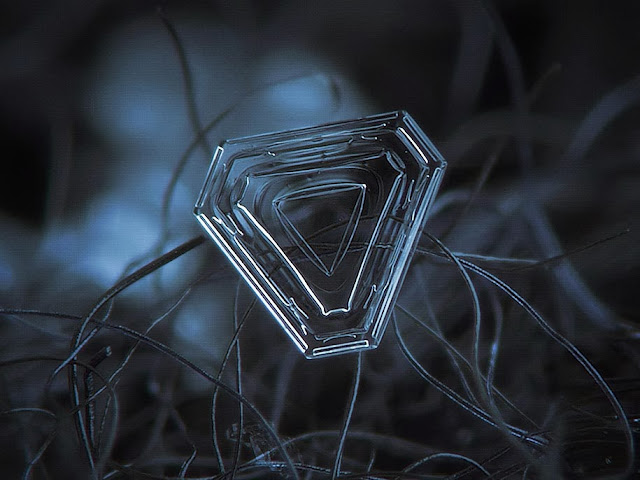
Crystallography: Snowflakes

Images shared via Alexey Kljatov.

A Russian photographer, Alexey Kljatov created a self made camera-lens combination to take some inexpensive photographs of snowflakes that clearly show the crystallographic structure of each flake.

With each flake having undergone different thermodynamics, no two flakes are alike. What is interesting is that each flake shows the basic most thermodynamic concepts with respect to crystallography at a macro level.

The dendrites grow spaced from each other like leafs on a branch instead of a single solid being frozen because, at the seed's surface and the part yet liquid (solid-liquid interface) at the center, the temperature higher than it is in the solid or liquid due to temperature inversion. This means not only the dendrites tend to equally space away from each other but also grow further away from the interface deep into the liquid depending on the time they get to freeze. This results in the dendrites growing in a pattern of branch and leaf like structure so well, almost as if it was calculated before it was made. Well not almost... it was naturally calculated before it formed. It's thermodynamics in action. During freezing the latent heat of fusion given away by the freezing material is being exchanged at the solid-liquid interface which results in inversion of temperature in this region. The inversion simply denotes the raise in temperature above the freezing point as well as the ambient liquid temperature at the interface. Instead of the inversion of temperature slowing down the process, it instead gives the process a pattern. The material does not wait for this temperature to lower down as it finds a freezing opportunity on as a separate dendrite. Crystal starts forming and growing in shape of dendrites. Depending on what the localized thermodynamic conditions were, each flakes forms in different sizes and shapes, which is remarkably shown in the photography.


Tuesday, November 19, 2013

Energy Harvesting: Self Sufficient Technologies

When we talk of going green, using solar, wind and other 'green' technologies, mostly we are unknowingly talking about energy harvesting. Harvesting energy from ambiance might be a solution that has been staring at us since a long time. We can totally eliminate the need for powering our electronics with external sources; batteries or fuel. There are a multitude of methods well within our capabilities.

Pakistan can take a great boost by starting with the small but numerous devices. The multitude of dry batteries that we import would not even be needed. A TV remote control can be powered by the same energy that we apply to press the 'button' if we use a piezoelectric material which converts the movement into enough voltage to send the signal. Powering handy devices with body heat, solar cells, piezoelectrics, or even use the excessive background noise that we have in form of radio waves and wifi signals on hundreds of channels to power devices.

On a macro-scale, The vast deserts are a good source of solar, wind and other forms of energy harvesting. Also, humans had always been having good living conditions prior to advent of electricity. Passive solar building design can take down the carbon foot print of a building to near zero.

It's time Pakistan takes steps towards such technologies. It might seem that highly developed nations develop such technologies and then it is transferred to us, but the truth is, most innovative and energy efficient technologies come from developing countries because they have to make do with the least possible resources. There is a huge range of technologies which were either developed for or by developing nations and later introduced to the developed ones.


As I explained in the last post about programmable materials, the processing of information is being decentralized to make it more viable... the power overload may not be any different from the information overload. The fact is, we do not need to reduce our energy consumption, we just need to reduce the wastage. Recycling and harvesting the wasted energy and making most devices self sufficient in regards to power is the obvious solution.

Sunday, October 6, 2013

Material Intelligence: The Programmable Matter

The new era is an epoch of smart materials where materials and non living things can have intelligence without any circuits, processing power, mechanical gadgets involved - it comes directly from the materials properties at nano-scale. Intelligent materials are being developed for a lot of purposes and include functionalities like:
  • Piezoelectric materials - convert vibrations to electricity and converse.
  • Shape memory alloys - remember their shape at temperature zones.
  • Magnetostrictive materials - reshape under magnetic influence and converse.
  • Magnetic shape memory alloys - change shape under significant magnetic field.
  • Magnetocaloric materials - reversibly change their temperature in ratio to magnetic field.
  • pH-sensitive polymers - change their volume with ambient pH.
  • Temperature responsive polymers - respond to temperature changes.
  • Halochromic materials - change colour with acidity.
  • Chromogenic systems - change colour with electricity, heat or light. LCDs use such materials.
  • Ferrofluids - strongly magnetizable fluids just by presence of magnetic field.
  • Photomechanical materials - change shape with light.
  • Polymorph materials - mold with hot water.
  • Self-healing materials - heal their own wear and tear.
  • Dielectric elastomers -  produce high strain with electricity.
  • Thermoelectric materials - convert temperature difference to electricity and converse.

This opens the doors to a new science of programming matter itself. Using any combination of materials above or other such materials it is possible to program the material to achieve basic functionalities that would normally take a computer processor or human brain to perform. A BBC news article mentions discovery of shape memory alloys that can be reshaped indefinitely by heating and cooling without wear and tear. The martensite structure of the shape memory alloys allows the materials to 'decide' conditionally and by the use of conditional programming of the materials they can be used to perform functions like automatic window openers or even as the means to guide solar panels on the Hubble Space Telescope to always point towards sun.

The programming of materials opens a front at nano-scale physics that uses the skills of computing and materials science to acquire results with no complexity at the macro level.

Thursday, September 19, 2013

Top 10 Space Weapons

While exotic weapons design and 'alien-ware' style weaponry is still a distant future but the speed our current technology and capabilities it is diversifying and moving towards that future is remarkable. Space.com lists top ten weapons that have yet been deployed by different nations to work from or in space as a form of space warfare to support operations on earth or a conflict in space. The list ranges from ICBMs, High altitude Non-nuclear EMPs, Cosmic satellites and China's satellite destroying missiles to Soviet Union's Almaz Space Station, DARPA's electromagnetism controlled stream of molten metal and the X-37B, the Orbital Vehicle with capabilities to throw Tungsten rods at targets on earth.

Read the the article on Top 10 Space Weapons for more.